


Self Bias
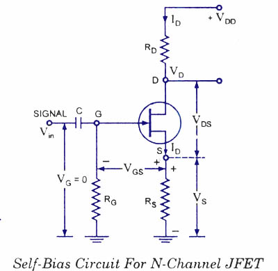
FET-Self Bias circuit
This is the most common method for biasing a JFET. Self-bias circuit for N-channel JFET is shown in figure.
Since no gate current flows through the reverse-biased gate-source, the gate current IG = 0 and, therefore,vG= iG RG = 0
With a drain current ID the voltage at the S is
Vs= ID Rs
The gate-source voltage is then
VGs = VG - Vs = 0 – ID Rs = – ID Rs
So voltage drop across resistance Rs provides the biasing voltage VGg and no external source is required for biasing and this is the reason that it is called self-biasing.
The operating point (that is zero signal ID and VDS) can easily be determined from equation and equation given below :
VDS = VDD – ID (RD + RS)
Thus dc conditions of JFET amplifier are fully specified. Self biasing of a JFET stabilizes its quiescent operating point against any change in its parameters like transconductance. Let the given JFET be replaced by another JFET having the double conductance then drain current will also try to be double but since any increase in voltage drop across Rs, therefore, gate-source voltage, VGS becomes more negative and thus increase in drain current is reduced.
No comments:
Post a Comment